
4.1 Diode concept and bias
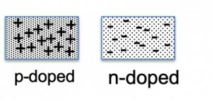
Diodes are two-terminal electronic devices made from semiconductor materials, such as silicon, or germanium, or from compound semiconductor materials, such as gallium-arsenide. Such materials have a conductivity lower than that of conductors, such as aluminum and copper, but larger than that of insulators such as glass and rubber. The conductivity of a semiconductor material can be increased substantially by a process of “doping” in which different types and amounts of impurity atoms are injected into the material to alter its number of free electric charges. An “n-type” material, characterized by an excess of electrons (negative charges) is created by adding an impurity such as phosphorus into the semiconductor material to increase its conductivity. A “p-type” material, characterized by a excess of “holes” (these can be thought of as empty sockets into which electrons can fit; they are positive charges), is created by adding a different type of doping impurity, such as boron to the semiconductor. The two doped materials have higher concentrations of free charges and therefore have higher conductivity than the intrinsic (non-doped) semiconductor material. For example, the conductivity of p-type silicon is five orders of magnitude higher than the conductivity of intrinsic silicon. refer back to chapter in resistance and conductivity
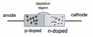
Semiconductor junction. A junction is created when n-type and p-type pieces of semiconductor material are brought together as illustrated in figure 4.5. Owing to the high concentration of holes (+) in the p-type region relative to the n-type region, some of the holes diffuse or travel across the junction into the n-type region. Likewise, some of the electrons diffuse across the junction from the n-type to the p-type region. Diffusing holes and electrons combine with each other near the junction, creating a depletion region characterized by an absence of free charges. The width of this junction can be influenced by applying an external voltage across the diode, and this regulates the amount of current that can flow through the device. Electrodes attached to the sides of the diode enable an external voltage to be applied. The electrode attached to the p-type region is called the anode, while the electrode attached to the n-type region is called the cathode.
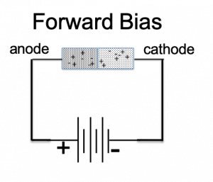
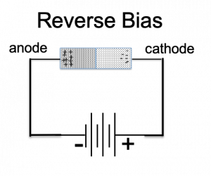
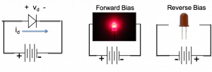
When an external voltage is applied across the diode, with a sufficiently high potential on the anode relative to the cathode, the diode is forward biased, and current flows through the device. Absent such an applied voltage, the diode is reverse biased, and current does not flow.
Forward bias. When a potential difference (voltage) is applied across the diode, with higher potential on the anode relative to the cathode, free negative charges from the n-type region are drawn toward the anode, while free positive charges from the p-type region are drawn toward the cathode. This fills in the depletion region with free charges, as depicted in figure 4.6, and enables current to flow through the device. Current flows from the anode to the cathode, with the amount of current being dependent upon the applied voltage. The voltage at which the depletion region is filled in, and current starts to flow, depends on the type of diode and the semiconductor materials used. For silicon and germanium rectifier diodes, this voltage is typically ~ 0.6V; for light emitting diodes (LEDs), the turn-on voltage typically ranges between ~1.5 and ~2.5V.
Reverse bias. When the applied voltage across the diode puts the anode at a potential lower than the cathode, positive charges in the p-region are drawn toward the anode, negative charges in the n-region are drawn toward the cathode, and the depletion region is widened, preventing current from flowing. This condition, depicted in figure 4.7, is referred to as reverse bias.
Diode schematic symbol. The schematic symbol for diode, shown in figure 4.8, resembles an arrow pointing from the anode to the cathode. This symbol helpfully reminds us that current flow through the diode is from anode to cathode. (It is also helpful to remember that current exits the cathode).

Diodes are used for multiple applications. Rectifier diodes are used in power supplies and other circuits, while light emitting diodes, or LED’s, are used in a variety of indicator lamps as well as in utility and decorative lighting and some biomedical instrumentation. When LED’s are forward biased, they emit photons at a wavelength determined by the semiconductors used. Reverse biased LED’s do not glow.
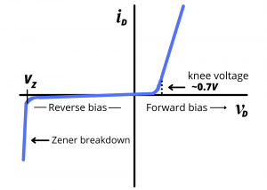
Diode  characteristic. Whereas a resistor is a linear two-terminal device (ie, it has a linear relationship) diodes are non-linear devices having a very different characteristic compared to a resistor. An example curve for a rectifier diode is shown below. Negligible current flows until the applied voltage across the diode is ~ 0.6 V (rectifier diode) or ~ 1.5V (LED); above this value, sometimes called the “knee” in the curve, current flows, and the amount of current depends on the applied voltage. At an applied voltage >0.7 volts (rectifier) or >2V (LED), the diode is forward biased, and large currents (10’s of mA to a few amps, depending on the diode) can flow. When the applied voltage is less than the knee voltage, very little current flows in the diode due to the impact of the reverse bias on the number of free charges discussed above. (When the reverse bias is large enough, valence electrons, normally bound to atoms within the semiconductor atomic lattice structure, are torn free from their bonds. These electrons then contribute to significant current flowing in the negative direction. This is referred to as breakdown, and special diodes called Zener diodes specifically designed to exploit this effect are sometimes used to set voltages in circuits.)
 curve, for a semiconductor diode
 and
and  are used for DC voltages and currents, while lower-case letters, such as
  and
and  are typically used to represent time-varying voltages and currents. This chapter contains numerous curves that characterize the current vs. voltage behavior for different types of diodes. Typically, these plots have their horizontal axis labeled
  for forward diode voltage (anode voltage – cathode voltage) and vertical axis labeled
  for diode forward current (flowing from anode to cathode). The curves can represent either DC (that is, non-changing) current vs. voltage relationships, or they can represent instantaneous values (values at a particular instant in time) of time-varying voltages and currents. Lower-case variable names are used on the plot axes since they are a more general representation than upper-case or capitalized letters. To make matters even more confusing, most of the diode circuits we will analyze will be DC circuits, and we will use capital letters, such as
  and
and  to refer to specific DC voltages and for these circuits. We will, therefore, see a mix of upper-case and lower-case variable namess in the plots, drawings, and circuit analyses in this chapter. If this presents a source of frustration or confusion, just remember that the plots all show the forward current through the diode versus the voltage drop across the diode and do not be overly concerned about the use of capitalized versus lower-case variable names.
