
5.1 Transistor Construction and Models
BJT composition. Bipolar junction transistors (BJT’s) are configured as NPN transistors, shown below, or as PNP transistors (not shown). The NPN transistor is comprised of three pieces of doped semiconductor, two n-type and one p-type, brought together to form a base-collector junction and a base-emitter junction. Recall the previous chapter’s discussion of semiconductor diodes where the relationship between voltage applied across and the resulting current through, a p-n junction was described. In that chapter, we learned that these junctions are characterized by forward or turn-on voltages, and these voltages can be modeled as voltage drops in equivalent circuit models.

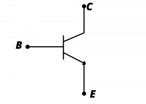
The schematic symbol for the transistor is a three-terminal device shown below. Often the base (B), collector (C) and emitter (E) are identified in a schematic symbol, but not always.
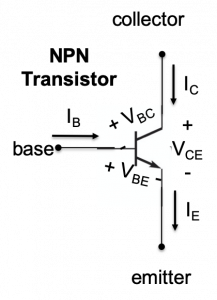
The following schematic identifies the base, collector and emitter as well as the currents through these terminals and the voltages across the three terminals.
Three BJT operating modes. Depending on the base current, the transistor operates in one of three modes, cutoff, active, or saturation, summarized in the table below. The table identifies the junction bias (forward or reverse) as well as the base, collector, and emitter currents, and the terminal voltages, for the three modes of operation.
Each of these modes can be characterized by an equivalent circuit that exhibits the junction voltages and currents summarized in the table. We examine these modes below.
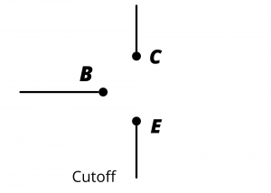
Transistor in cutoff. When the base current is zero and the base-emitter voltage  the transistor is in the cutoff region. The base-emitter and base-collector junctions are both reverse-biased, and no current flows through through any of the three terminals. A transistor is off in this mode and the circuit model is characterized by open circuits between all three terminals.
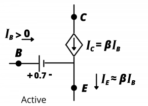
Transistor in active region. In the active mode, the base-emitter junction is forward biased, while the base-collector junction is reverse biased. When a positive current  flows into the base of the transistor, the transistor turns on, permitting current to flow between the collector and the emitter terminals. In the active region, the collector current is proportional to the base current, and the proportionality constant,
  , is a characteristic of the transistor. Thus,
  . Values for typically range between 20 and 200, depending on the transistor chosen. If we were to apply KCL to the entire transistor (treating the device as a single node, for which conservation of charge applies), we see that
  . This is due to the fact that and
  are both drawn as currents entering the transistor, while
  is drawn exiting the transistor. Since , we have
  . Thus, in the active mode, we find that one current, flows into the base and out of the emitter, while another current,
  simultaneously flows into the collector and out of the emitter. Since is typically large, we can approximate ≈. The transistor thus behaves as a current amplifier, where the collector-to-emitter current is an amplified version of the base current. The current flow between the collector and the emitter is in direct proportion to the base current, and the transistor behaves as a current amplifier.
Transistor in the saturation region. Increasing the base current beyond a certain point results in flattening or decrease of the transistor gain, such that further increases in can not be met with corresponding further increases in , and we find that the collector current  . When this happens, both the base-emitter junction and the base-collector junction are both forward biased, and the transistor is said to be in saturation. Importantly, the voltage drop between the collector and emitter is small, typically,
  , and the transistor behaves like an “on” switch between the collector and the emitter.

